AR1010 Pic Basic Program for FM Radio
By: Don McClatchie
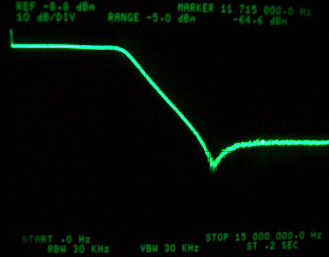
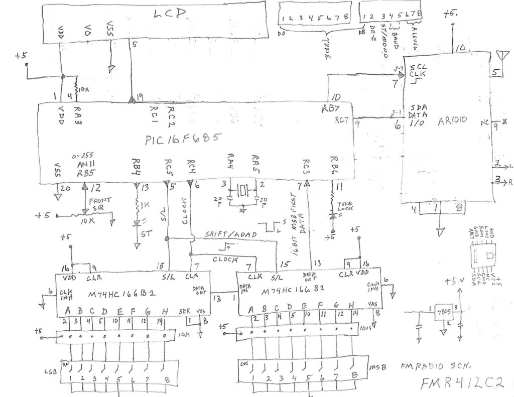
This is for those who have been trying to make an AR1010 sub-board work using PIC BASIC Pro and a Pic Microcontroller. I was not able to find any examples of BASIC programming for this neat little radio sub-board using the AR1010 from AIROHA Technology Corp. This system uses two 8 position switches to select the 9 bit FM channel, 1 bit De-Emphasis, 1 bit Mono/Stereo, 2 bit Band, and 3 bit Audio Level output. This is just a working example of Pic BASIC programming to help anyone trying to make their project work. The switch selections are multiplexed into the Pic Microcontroller using two M74HC166B1 Parallel to Serial converter chips. There is an LCD to read internal registers for testing and development. Here is the schematic. This may not be the best way to program this, but it will get the AR1010 hart started and play the music.
‘*****************************************************************************
‘* Name : FMR412C2.BAS *
‘* Author : Don McClatchie *
‘* Notice : Copyright (c) 2022 FM SYSTEMS, INC *
‘* : All Rights Reserved *
‘* Date : 5/16/2022 *
‘* Version : 2.0 Two Wire Communications AR1010 Sub-Board A15-45-B-04 *
‘* Notes : FM Stereo Receiver using AR1010 Module 76 to 108 Mhz FM Band *
‘* : Selectable De-Emphasis,Band,Stereo/Mono,Squelch,& Audiolevel *
‘*****************************************************************************
; PBP -p16f685
;@_CONFIG_HS_OSC ; OSC External 20MHz
;@_CONFIG_WDT_ON ; WatchDog Timer ON
;@_CONFIG_PWRT_ON ; Power Up Timer ON
;@_CONFIG_MCLR_OFF ; MCLR as I/O
;@_CONFIG_BOD_ON ; Brown Out Detector ON
;@_CONFIG_PROTECT_ON ; Code Protect ON
;@_CONFIG_CPD_ON ; Memory Protect ON
include “modedefs.bas”
; Set-Up I/O Pins
trisA = %000000 ; Set all pins to output
trisB = %00100000 ; Set All Outputs Except Pin 12
trisC = %00000000 ; Set Pins All Output Except Pin 7
ANSEL = %00000000 ; AN0-AN7 Analog Off
ANSELH = %00000100 ; AN11 Pin 12 Analog Other Pins Digital
ADCON0 = %00101101 ; Left Justified Vref Pin 12
ADCON1 = %00100000 ; A/D Conversion Clock Focs/32
; Defines
DEFINE OSC 20 ; Set oscillator for 20MHz
define ser2_bits 8 ; Set Serial Data Bits to 8
define ADC_bits 10 ; ADC to 10 Bits
define ADC_CLOCK 3 ; Clock Source RC
define ADC_SAMPLEUS 50 ; ADC Sample Time in uS
; Variables
W0 var word ; Saved Switch Data
W1 var word ; S1/S2 Saved Switch Data Variable
TUNE var word ; 9 Bit Tuning Select Variable S1-1-8 S2-1
Alev var Byte ; Audio Level Selector Variable S2-6-8
DATA1 var byte ; Read Data Variable
DATA2 var byte ; Read Data Variable
DATA3 var word ; Read Data Variable
DATA4 var byte ; Read Data Variable
CNT var word ; Squelch Pot Variable Temp used for loop
TT var word ; Used for display temp
AR1 var word ; AR1 Register
AR2 var word ; AR2 Register
AR3 var word ; AR3 Register
RSSIL var word ; AR11 Low Side Injection Word
RSSIH var word ; AR11 High side Injection Word
AR14 var word ; AR14 Register
VOL2VOL var byte ; Audio Level Variable
AR2CLR var byte ; AR2 Clear Register (tune bit)
AR2SET var byte ; AR2 Set Register (tune bit)
AR11SET var word ; AR11 Hilow Injection Variable
AR11L var word
AR11H var word
; Constants
AR11L = %0100111101010000
AR11H = %1100111111010101
; Presets
Clear ; Clear All Variables
pause 1000 ; Pause for Start Up and LCD
Start1: ; Main Program Initial Data Read
PortA.0 = 0 ; LCD Data Line to 0
PortC.7 = 1 ; AR1010 SDA Data Line to 1
PortB.7 = 0 ; AR1010 SCL Clock Line to 1
PortC.5 = 1 ; M74HC166B1 Shift/Load to Shift
PortC.4 = 0 ; M74HC166B1 Clock Low
gosub SCANLOAD ; Scan and Load Switch Data
ASSIGN: ; Assign Tune Switchs
Tune.0 = W0.bit0 ; Get 0 bit from SW Data for Tune
Tune.1 = W0.bit1 ; Get 1 bit from SW Data for Tune
Tune.2 = W0.bit2 ; Get 2 bit from SW Data for Tune
Tune.3 = W0.bit3 ; Get 3 bit from SW Data for Tune
Tune.4 = W0.bit4 ; Get 4 bit from SW Data for Tune
Tune.5 = W0.bit5 ; Get 5 bit from SW Data for Tune
Tune.6 = W0.bit6 ; Get 6 bit from SW Data for Tune
Tune.7 = W0.bit7 ; Get 7 bit from SW Data for Tune
Tune.8 = W0.bit8 ; Get 8 Bit from SW Data for Tune
AR1 = %0101101100000101 ; Preset AR1.byte1 0101101100000101
AR1.bit4 = W0.bit9 ; De-Emphasis S2 bit4 75uS = 1 50uS = 0
AR1.bit3 = W0.bit10 ; Stereo/Mono S2 bit3 Mono = 1 Stereo = 0
AR2 = %1101000010111001 ; Preset AR2 1101000010111001
AR2.byte0 = Tune ; Add Low byte of tune
AR2CLR = 208 ; Byte1 bit1 = 0 TUNE off
AR2SET = 210 ; Byte1 bit1 = 1 TUNE on
AR2CLR.bit0 = W0.bit8 ; Add 9th bit to tune off
AR2SET.bit0 = W0.bit8 ; Add 9th bit to tune on
AR3 = %1010000000010000 ; Default seekup,seek,space,band,vol,seekth
AR3.bit12 = W0.bit11 ; Band bit1
AR3.bit11 = W0.bit12 ; Band bit0
ALEV.bit0 = W0.bit13 ; SW2-6 Audio Level Bit0
ALEV.bit1 = W0.bit14 ; SW2-7 Audio Level Bit1
Alev.bit2 = W0.bit15 ; SW2-8 Audio Level Bit2
; VOL2 VOL
if Alev = 0 then VOL2VOL = 15 ; +0 0000;1111 Turns 3bits into 4bits 7 Select
if Alev = 1 then VOL2VOL = 75 ; +4 0100;1011
if Alev = 2 then VOL2VOL = 251 ; +6 1111,1011
if Alev = 3 then VOL2VOL = 249 ; +8 1111,1001
if Alev = 4 then VOL2VOL = 247 ; +10 1111,0111
If Alev = 5 then VOL2VOL = 230 ; +12 1110,0110
if Alev = 6 then VOL2VOL = 113 ; +14 1110,0011
if Alev = 7 then VOL2VOL = 240 ; +18 1111,0000
AR3.bit10 = VOL2VOL.bit3 ; Volume Bit3 SW2-8
AR3.bit9 = VOL2VOL.bit2 ; Volume Bit2 SW2-7
AR3.bit8 = VOL2VOL.bit1 ; Volume Bit1 SW2-6
AR3.bit7 = VOL2VOL.bit0 ; Volume Bit0
AR14 = %1111110000101101 ; AR14 Default Register
AR14.bit15 = VOL2VOL.bit7 ; Volume2 Bit3
AR14.bit14 = VOL2VOL.bit6 ; Volume2 Bit2
AR14.bit13 = VOL2VOL.bit5 ; Volume2 Bit1
AR14.bit12 = VOL2VOL.bit4 ; Volume2 Bit0
W1 = W0 ; Load Switch Data to store for change
REGISTERLOAD: ; Registerload Routine 1=READ 0=WRITE
gosub STARTCLK ; Start Clock Sequence
gosub ARADD ; Go to Chip Address Send Routine
shiftout PortC.7,PortB.7,1,[1] ; Write Address R1 De-E
gosub WRITEACK ; Send Ack Clock Pulse + Receive ACK
shiftout PortC.7,PortB.7,1,[AR1.byte1] ; Write Data D15-D8 01011011
gosub WRITEACK ; Send Ack Clock Pulse + Receive ACK
shiftout PortC.7,PortB.7,1,[AR1.byte0] ; Write Data D7-D0 00010101 = no mute
gosub WRITEACK ; Send Ack Clock Pulse + Receive ACK
gosub STOPCLK ; Send Stop Comm to AR1010
gosub STARTCLK ; Start Clock Sequence
gosub ARADD ; Go to Chip Address Send Routine
shiftout PortC.7,PortB.7,1,[2] ; Write Address R2 Tune
gosub WRITEACK ; Send Acknowledge Clock Pulse
shiftout PortC.7,PortB.7,1,[AR2SET] ; Write Data D15-D8 Tune HBits 11000110
gosub WRITEACK ; Send Acknowledge Clock Pulse
shiftout PortC.7,PortB.7,1,[tune.byte0] ; Write Data D7-D0 Tune Lbyte 11000110
gosub WRITEACK ; Send Acknowledge Clock Pulse
gosub STOPCLK ; Send Stop Comm to AR1010
gosub STARTCLK ; Start Clock Sequence
gosub ARADD ; Go to Chip Address Send Routine
shiftout PortC.7,PortB.7,1,[3] ; Write Address R2 Tune
gosub WRITEACK ; Send Acknowledge Clock Pulse
shiftout PortC.7,PortB.7,1,[AR3.byte1] ; Write Data D15-D8 Tune HBits 10100111
gosub WRITEACK ; Send Acknowledge Clock Pulse
shiftout PortC.7,PortB.7,1,[AR3.byte0] ; Write Data D7-D0 Tune LowBits00010000
gosub WRITEACK ; Send Acknowledge Clock Pulse
gosub STOPCLK ; Send Stop Comm to AR1010
gosub STARTCLK ; Start Clock Sequence
gosub ARADD ; Go to Chip Address Send Routine
shiftout PortC.7,PortB.7,1,[10] ; Write Address R10 Seek_wrap
gosub WRITEACK ; Send Acknowledge Clock Pulse
shiftout PortC.7,PortB.7,1,[%10000010] ; Write Data D15-D8 10000010
gosub WRITEACK ; Send Acknowledge Clock Pulse
shiftout PortC.7,PortB.7,1,[%11001110] ; Write Data D7-D0 seek_wrap 11001010
gosub WRITEACK ; Send Acknowledge Clock Pulse
gosub STOPCLK ; Send Stop Comm to AR1010
gosub STARTCLK ; Start Clock Sequence
gosub ARADD ; Go to Chip Address Send Routine
shiftout PortC.7,PortB.7,1,[11] ; Write Address R11 hilo_side
gosub WRITEACK ; Send Acknowledge Clock Pulse
shiftout PortC.7,PortB.7,1,[%01001111] ; Write Data D15-D8 11001111
gosub WRITEACK ; Send Acknowledge Clock Pulse
shiftout PortC.7,PortB.7,1,[%01010101] ; Write Data D7-D0 01010101
gosub WRITEACK ; Send Acknowledge Clock Pulse
gosub STOPCLK ; Send Stop Comm to AR1010
gosub STARTCLK ; Start Clock Sequence
gosub ARADD ; Go to Chip Address Send Routine
shiftout PortC.7,PortB.7,1,[14] ; Write Address R14 Volume
gosub WRITEACK ; Send Acknowledge Clock Pulse
shiftout PortC.7,PortB.7,1,[AR14.byte1] ; Write Data D15-D8 Volume 11111111
gosub WRITEACK ; Send Acknowledge Clock Pulse
shiftout PortC.7,PortB.7,1,[AR14.byte0] ; Write Data D7-D0 00000000
gosub WRITEACK ; Send Acknowledge Clock Pulse
gosub STOPCLK ; Send Stop Comm to AR1010
gosub STARTCLK ; Start Clock Sequence
gosub ARADD ; Go to Chip Address Send Routine
shiftout PortC.7,PortB.7,1,[0] ; Write Address R1 xo_en/Enable
gosub WRITEACK ; Send Acknowledge Clock Pulse
shiftout PortC.7,PortB.7,1,[%11111111] ; Write Data D15-D8 11111111
gosub WRITEACK ; Send Acknowledge Clock Pulse
shiftout PortC.7,PortB.7,1,[%11111011] ; Write Data D7-D0 Set Enable 11111011
gosub WRITEACK ; Send Acknowledge Clock Pulse
gosub STOPCLK ; Send Stop Comm to AR1010
pause 1000 ; Pause 1 S
for CNT = 0 to 1 ; Clear Squelch Variable
TUNE2: ; Tuning Routine
gosub STARTCLK ; Start Clock Sequence
gosub ARADD ; Go to Chip Address Send Routine
shiftout PortC.7,PortB.7,1,[1] ; Write Address R1
gosub WRITEACK ; Send Acknowledge Clock Pulse
shiftout PortC.7,PortB.7,1,[AR1.byte1] ; Write Data D15-D8 01011011
gosub WRITEACK ; Send Acknowledge Clock Pulse
shiftout PortC.7,PortB.7,1,[AR1.byte0] ; Write Data D7-D0 Set Hmute 00010111
gosub WRITEACK ; Send Acknowledge Clock Pulse
gosub STOPCLK ; Send Stop Comm to AR1010
gosub STARTCLK ; Start Clock Sequence
gosub ARADD ; Go to Chip Address Send Routine
shiftout PortC.7,PortB.7,1,[2] ; Write Address R1 Tune
gosub WRITEACK ; Send Acknowledge Clock Pulse
shiftout PortC.7,PortB.7,1,[AR2CLR] ; Write Data D15-D8 Clear Tune bit
gosub WRITEACK ; Send Acknowledge Clock Pulse
shiftout PortC.7,PortB.7,1,[TUNE.byte0] ; Write Data D7-D0 Load Tune bits
gosub WRITEACK ; Send Acknowledge Clock Pulse
gosub STOPCLK ; Send Stop Comm to AR1010
gosub STARTCLK ; Start Clock Sequence
gosub ARADD ; Go to Chip Address Send Routine
shiftout PortC.7,PortB.7,1,[3] ; Write Address R3 Seekup
gosub WRITEACK ; Send Acknowledge Clock Pulse
shiftout PortC.7,PortB.7,1,[AR3.byte1] ; Write Data D15-D8 Clr seek bit
gosub WRITEACK ; Send Acknowledge Clock Pulse
shiftout PortC.7,PortB.7,1,[AR3.byte0] ; Write Data D7-D0 00000000
gosub WRITEACK ; Send Acknowledge Clock Pulse
gosub STOPCLK ; Send Stop Comm to AR1010
gosub STARTCLK ; Start Clock Sequence
gosub ARADD ; Go to Chip Address Send Routine
shiftout PortC.7,PortB.7,1,[2] ; Write Address R3 Seekup
gosub WRITEACK ; Send Acknowledge Clock Pulse
shiftout PortC.7,PortB.7,1,[AR2CLR] ; Write Data D15-D8 11010010
gosub WRITEACK ; Send Acknowledge Clock Pulse
shiftout PortC.7,PortB.7,1,[TUNE.byte0] ; Write Data D7-D0 Volume 11001011
gosub WRITEACK ; Send Acknowledge Clock Pulse
gosub STOPCLK ; Send Stop Comm to AR1010
gosub STARTCLK ; Start Clock Sequence
gosub ARADD ; Go to Chip Address Send Routine
shiftout PortC.7,PortB.7,1,[2] ; Write Address R0 xo_en/Enable
gosub WRITEACK ; Send Acknowledge Clock Pulse
shiftout PortC.7,PortB.7,1,[AR2SET] ; Write Data D15-D8 11111111
gosub WRITEACK ; Send Acknowledge Clock Pulse
shiftout PortC.7,PortB.7,1,[TUNE.byte0] ; Write Data D7-D0
gosub WRITEACK ; Send Acknowledge Clock Pulse
gosub STOPCLK ; Send Stop Comm to AR1010
gosub STARTCLK ; Start Clock Sequence
gosub ARADD ; Go to Chip Address Send Routine
shiftout PortC.7,PortB.7,1,[1] ; Write Address R3 Seekup
gosub WRITEACK ; Send Acknowledge Clock Pulse
shiftout PortC.7,PortB.7,1,[%01011011] ; Write Data D15-D8
gosub WRITEACK ; Send Acknowledge Clock Pulse
shiftout PortC.7,PortB.7,1,[%00010101] ; Write Data D7-D0 Clr Hmutebit00010101
gosub WRITEACK ; Send Acknowledge Clock Pulse
gosub STOPCLK ; Send Stop Comm to AR1010
pause 100 ; Pause 1S
DATA1 = 0 ; Clear Data1 Variable
DATA2 = 0 ; Clear Data2 Variable
DATA3 = 0 ; Clear Data3 Variable
DATA4 = 0 ; Clear DATA 4 Variable
READ1: ; Read Register Data
gosub STARTCLK ; Start Clock Sequence
gosub ARADD ; Send 7bit Slave Address + 0 Write(32)
shiftout PortC.7,PortB.7,1,[18] ; Write Address from switches (READ)
gosub WRITEACK ; Send Acknowledge Clock Pulse REC
gosub STARTCLK ; Start Clock Sequence Again
shiftout PortC.7,PortB.7,1,[33] ; Send 7bit Slave Address + 1 READ(33)
gosub WRITEACK ; Send Acknowledge Clock Pulse REC
shiftin PortC.7,PortB.7,0,[DATA1] ; Clock in High Byte Data from AR1010
trisC.bit7 = 0 ; Make PortC.7 an Output
gosub READACK ; Send READ Acknowledge to AR1010
shiftin PortC.7,PortB.7,0,[DATA2] ; Clock in Low Byte Data from AR1010
trisC.bit7 = 0 ; Make PortC.7 an Output
gosub READACK ; Send READ Acknowledge to AR101
gosub STOPCLK ; Send Stop Com to AR1010
READ2: ; Read Register Data
gosub STARTCLK ; Start Clock Sequence
gosub ARADD ; Send 7bit Slave Address + 0 Write(32)
shiftout PortC.7,PortB.7,1,[19] ; Write Address from switches (READ)
gosub WRITEACK ; Send Acknowledge Clock Pulse REC
gosub STARTCLK ; Start Clock Sequence Again
shiftout PortC.7,PortB.7,1,[33] ; Send 7bit Slave Address + 1 READ(33)
gosub WRITEACK ; Send Acknowledge Clock Pulse REC
shiftin PortC.7,PortB.7,0,[DATA3.byte0] ; Clock in High Byte Data from AR1010
trisC.bit7 = 0 ; Make PortC.7 an Output
gosub READACK ; Send READ Acknowledge to AR1010
shiftin PortC.7,PortB.7,0,[DATA4] ; Clock in Low Byte Data4 from AR1010
trisC.bit7 = 0 ; Make PortC.7 an Output
gosub READACK ; Send READ Acknowledge to AR101
gosub STOPCLK ; Send Stop Com to AR1010
pause 100 ; Pause for STC
next ; Do it again
if DATA4.bit5 <> 1 then goto TUNE2 ; Go back if STC Flag not set
If DATA2 < 150 then goto TUNE2 ; Read Data2 for IF-CNT re-tune if low
; Compute Channel Frequency Routine
DATA3 = DATA3 *2 ; Test for display Channel
If DATA4 > 128 then DATA3 = DATA3 + 1 ; test for display Channel
if DATA4 > 128 then DATA4 = DATA4 – 128 ; test for display Channel
DATA3 = DATA3 + 690 ; test for display Channel
Main: ; Main Loop
gosub SCANLOAD ; Get Switch Settings
if W0 = W1 then PortB.6 = 0 ; test if Sw is changed
if W0 <> W1 then PortB.6 = 1 ; LED off if switch changed until lock
If W0 <> W1 then goto START1 ; Go back if Switch has changed
if DATA4.bit3 = 1 then PortB.4 = 1 ; Stereo Led ON
if data4.bit3 = 0 then PortB.4 = 0 ; Stereo Led Off
If DATA4.bit4 = 1 then goto START1 ; Check STC flag = 1 Seektune Complete
; LCD READOUT Routine for Testing
ADCIN 11, SQL ; Get Squelch knob Analog level
serout2 PortA.0, 16416, [254,88] ; Send LCD Clear
serout2 PortA.0, 16416, [254,71,1,1] ; Select 1rst Row of LCD
serout2 PortA.0, 16416, [“18D1 “,#DATA1,” D2 “,#DATA2] ;Send 1rst Row to LCD
serout2 PortA.0, 16416, [254,71,1,2] ; Select 2nd Row of LCD
serout2 PortA.0, 16416, [“19D3 “,#DATA3,” D4 “,#DATA4] ;Send 2nd row DATA to LCD
Pause 100 ; pause (display flash) to see in loop
goto Main ; Loop main program
ARADD: ; Subroutine to send chip address
shiftout PortC.7,PortB.7,1,[32] ; Write AR1010 Address + Write 32
trisC.bit7 = 1 ; Make PortC.7 an Input
PortB.7 = 0
PortB.7 = 1 ; Clock Line High
pauseus 2 ; Wait 1 uS
PortB.7 = 0 ; Clock Line Low
trisC.bit7 = 0 ; Make PortC.7 an Output
return ; go back
STARTCLK: ; AR1010 Start Clock Routine
PortB.7 = 1 ; Clock Line High
PortC.7 = 1 ; Data Line High
pauseus 2 ; Wait 2 uS
PortC.7 = 0 ; Data Line Low
pauseus 2 ; Wait 2 uS
PortB.7 = 0 ; Clock line Low
return ; Go back
STOPCLK: ; AR1010 Stop Clock Routine
PortC.7 = 0 ; Data Line Low
pauseus 2 ; Wait 2 uS
PortB.7 = 1 ; Clock line High
pauseus 2 ; Wait 2 uS
PortC.7 = 1 ; Data Line High
return ; Go back
READACK: ; READ Acknowledge Routine
PortC.7 = 0 ; Data Line Low
PortB.7 = 1 ; Clock Line High
pauseus 1 ; Wait 1 uS
PortB.7 = 0 ; Clock Line Low
PortC.7 = 1 ; Data Line High
return ; Go Back
WRITEACK: ; Write Acknowledge Routine
trisC.bit7 = 1 ; Make PortC.7 an Input
PortB.7 = 0 ; Clock Line Low
PortB.7 = 1 ; Clock Line High
pauseus 2 ; Wait 1 uS
PortB.7 = 0 ; Clock Line Low
trisC.bit7 = 0 ; Make PortC.7 an Output
Return ; Go Back
SCANLOAD: ; SCANLOAD Read Switch Routine
PORTC.5 = 0 ; Shift/Load to Load
PORTC.4 = 0 ; Clock Low
PORTC.4 = 1 ; Clock High
PORTC.4 = 0 ; Clock Low
PORTC.5 = 1 ; Shift/Load to Shift
PORTC.5 = 1 ; Shift/Load to Shift
shiftin PORTC.3, PORTC.4, 0, [W0\16] ; Receive Data from Switchs 16 bit
trisC.bit7 = 0 ; Make Data Line PortC.7 an output
Return ; go back
end ; end